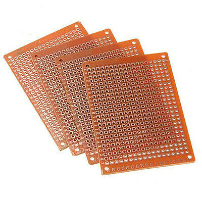
PCB Proto Board 150mmx90mm
R16.00
PCB Proto Board 150mmx90mm Printed circuit boards use conductive tracks to connect components, are an essential step in an electrical item.
70 in stock
PCB Proto Board 150mmx90mm
PCB Proto Board 150mmx90mm A prototype printed circuit board is an essential step in the design process of an electrical item.
Printed circuit boards use conductive tracks to connect components. Printed circuit boards have lower manufacturing costs that traditional circuit boards
WHAT IS A PROTOTYPE PCB BOARD?
A prototype printed circuit board is an essential step in the design process of an electrical item. Printed circuit boards use conductive tracks to connect components.
Printed circuit boards have lower manufacturing costs that traditional circuit boards. Because they are printed, there is no need for a complex wiring process.
Electronic design businesses can benefit from faster turnaround time, as the manufacturing process for a PCB is far less labor-intensive than traditional circuit boards.
Due to the lack of wiring, PCBs are safer and more reliable. They are also less pross to short-circuits. Using PCBs also prevents wires from snapping or breaking loose.
WHAT IS THE DIFFERENCE BETWEEN PROTOTYPE PCBS AND SOLDERLESS BREADBOARDS?
A solderless breadboard is a useful tool in electronics development. Solderless breadboards have been in use since the 1970s.
Breadboards consist of a grid of spring-loaded clips that allow the electrical connections.
Breadboards are temporary and can be reused for other designs, making them a handy tool in prototyping. They can be used to test the functions of a particular design before a printed circuit board can be made up later.
Breadboards have some limitations. They’ll only work with through-hole components, whereas a printed circuit board will typically use surface-mount components.
While a breadboard can be useful for specific circuits, it can cause problems in using breadboards as a meaningful prototype because of the lack of surface-mounted components.
In most cases, modern circuitry should have prototype PCBs made up rather than settling for a breadboard prototype.
HOW IS A CIRCUIT BOARD MADE UP?
There are several types of circuit boards. The most common are single-sided and have copper tracks connecting the components on one side of the PCB. These are called one layer PCBs, although you can also find double-sides PCBs and multi-layered PCBs.
Several elements make a printed circuit board. These include FR4, copper, solder mask, and silkscreen.
FR4
FR stands for “flame retardant.” FR4 is a glass-reinforced epoxy resin laminate. This is the main element of the circuit board, and it is also the part that gives it rigidity.
Copper
Copper is laminated to the board. This process involves heat and adhesive. The number of copper plates used will determine whether the board is a one-layer PCB, whether it is double-layered, or multi-layered.
Soldermask
The solder mask layer is in place to insulate the copper traces. This prevents solder jumpers and keeps the copper from coming into contact with other metal.
Silkscreen
The final layer on a printed circuit board is the silkscreen layer. This is used to print letters and numbers onto the PCB to aid in the assembly process. Although white is the most common choice, any color can be used.
WHAT IS THE PCB MANUFACTURING PROCESS?
There are two different types of processes used in the fabrication of printed circuit boards; these include through-hole and surface mounted.
Through-hole technology uses leads inserted into holes on one side of the circuit board.
These are then soldered to the copper layer on the opposite side.
Surface-mounted technology is directly soldered onto the board.
There is no need to use leads.
The advantage of surface mounting technology over through-hole boards is that you can create smaller PCBs with the ability to carry out more complicated processes.
Only logged in customers who have purchased this product may leave a review.
Related products
Arduino
Reviews
There are no reviews yet.